RISC-V CPU & CUSTOM GPU ON AN FPGA PART 9 – A LARGER BIOS, CLOCK GENERATION AND ACTUAL INSTRUCTIONS
BEFORE WE BEGIN
In this part we’ll increase our BIOS and use an updated ROM image, talk about clocks and make NekoIchi run some code.
But before we go further, and since the files are getting too large to post here, we need to grab them from a git repository. Please head over to https://github.com/ecilasun/nekoichiarticle and use the following command to pull the files for all parts of the series:
git clone https://github.com/ecilasun/nekoichiarticle.gitafter creating and changing to a folder of your preference with sufficient free disk space, since this is where we’ll be working on all parts of the series from now on.
NOTE: A small change done starting in this part to the project brings us a nicely arranged include file, namely cpuops.vh, which contains all the instruction groups and CPU states so we can refer to them from the decoder and the cpu itself without having to pollute our code with inline defines.
MMCM and Larger BIOS
An MMCM is a built in module on Xilinx parts which can generate a variety of clock signals by means of division or multiplication of that signal to create different phases and frequencies of clock signals.
There are usually several MMCM units on an FPGA. This is to our advantage, as we can use two MMCMs at different corners of the FPGA to feed independent clock signals to different modules in our design.
For now, we have one clock signal, but we’ll use an MMCM for another purpose: to get a proper startup reset behavior.
The MMCM has an output signal, usually named ‘locked’. This signal tells us when the output clock is stable and usable. Once we integrate this with our hardware reset button, we can get a design that receives its reset signal from not only the reset button, but also from the MMCM, thus waiting in reset state properly until the clock is running properly.
Easiest way to add one to our project is via the Clocking Wizard IP generator. The project files have already been added on github for part9, where you can find the new full setup of our top module which uses the new clock generator.
`timescale 1ns / 1ps

module nekotop(
	// Input clock
	input CLK_I,
	// Reset on lower panel, rightmost button
	input RST_I,
	// 4 monochrome LEDs
	output [3:0] led
);

clockgen myclock(
	.resetn(~RST_I),		// Incoming external reset (negated)
	.clk_in1(CLK_I),		// Input external clock
	.cpuclock(cpuclock),	// Generated CPU clock
	.locked(clockLocked) );	// High when clock is stable

wire reset_p = RST_I | (~clockLocked);
wire reset_n = (~RST_I) & clockLocked;

wire [3:0] diagnosis;

// Full 32 bit BYTE address between CPU and RAM
wire [31:0] memaddress;
// Data wires from/to CPU to/from RAM
wire [31:0] cpudataout;
wire [31:0] cpudatain;
wire [3:0] cpuwriteena;

sysmem mymemory(
	.addra(memaddress[17:2]),	// 16 bit DWORD address
	.clka(cpuclock),		// Clock, same as CPU clock
	.dina(cpudataout),		// Data in from CPU to RAM address
	.douta(cpudatain),		// Data out from RAM address to CPU
	.ena(reset_n),			// Reads enabled only when not in reset
	.wea(cpuwriteena) );		// Write control line from CPU

riscvcpu mycpu(
	.clock(cpuclock),		// CPU clock
	.reset(reset_p),		// CPU reset line
	.diagnosis(diagnosis),		// Diagnosis output
	.memaddress(memaddress),	// Memory address to operate on
	.cpudataout(cpudataout),	// CPU data to write to external device
	.cpuwriteena(cpuwriteena),	// Write control line
	.cpudatain(cpudatain) );	// Data from external device to CPU

assign led = diagnosis;

endmodule
Another thing to note here is that we now have changed our block memory device to a much larger (65536 DWORDs wide) unit, addressed by 16bit DWORD indices, and are now passing the full byte address out from the CPU instead of truncating it. This will become handy if you wish to add devices that actually accept byte addresses later on.
Adding new instuctions
Actually, this is fairly straightforward. All we need to do is to decide on a few things in our decoder and pass the decisions out to the CPU:
- Does this instruction write back to a register?
- Does this instruction set up an ALU operation?
- Does this instruction decide on a branch?
If you check the decoder.sv file, you’ll see that it now checks each instruction type and will decide on what ALU op to use, and whether we should write back to the destination register, in addition to the previous parts it was decoding. The register write enable is sometimes omitted, for instance in the LOAD operation, where it is beneficial to delay it further to its own dedicated state (since LOAD has delay cycles due to the memory device and should not keep write line open at all times)
Branch ALU
Another new module that we acquire in this part is the branch ALU. It is very similar to the ALU, but instead of doing math operations, it produces a single bit value which tells us whether to take the current branch or not. It’s currently driven by the decoder, and its output is used in the EXEC state on our cpu if we’re running a branch operation, to select either the current PC + 4, or the branch target as our nextPC.
CPU EXEC State
The riscvcpu.sv file has been expanded to include the above new units, clock signals and wider data wires, as well as a memory write control signal. Also, it includes three new states: a LOADSTALL state to wait for memory reads, a LOADCOMPLETE state to trigger writes back to registers, and a STORE state.
The EXEC state has also been expanded. It now checks the decoder output ‘opcode’ to decide on the next CPU state to fall to, and set up memory address, nextPC and/or write control lines to memory.
If you were to check our RISC-V ISA Spec, you’ll find that RISC-V never reads or writes to memory except for the LOAD and STORE instructions. In our CPU implementation, these instructions are trapped and run through their own dedicated states, which also guarantees that we don’t collide with the memory read operations coming from the instruction fetching mechanism.
You’ll find that the FENCE and SYSTEM instructions are currently fall-through, and do nothing. The SYSTEM instruction will be quite densely populated in another part of this series, but for now we keep these two unoccupied to keep our focus sharp.
A common thing you’ll notice in the code base is that some registers appear to get written twice. For instance:
cpustate[`CPUEXEC]: begin
	// We decide on the nextPC in EXEC
	nextPC <= PC + 32'd4;
...
unique case (opcode)
	`OPCODE_JAL: begin
...
		nextPC <= PC + immed;
...
	end
This is intentional. The idea here is that the nextPC <= PC+32’d4 is our default behavior, and will be used for all cases except where we intentionally use some other value, as in the JAL instruction. In short, when you see parallel assignment operations (<=) in code, the behavior is that the last write to the same register is the final value of that register. This means in the JAL case, nextPC will only be set to PC+immed and there should not be any conflicts in behavior.
But you might think, if that’s the case, why don’t we set the cpustate[] once as well? The reason is that cpustate bits are cleared at start, and only one is set. If we were to go ahead and set the RETIRE bit at the top of our case statement, and then change our mind in the LOAD instruction and set LOADSTALL bit for instance, that would end up setting two bits simultaneously, causing undesired behavior on the next clock. So for one-hot encoding, in this code base at least, I prefer to clear all bits once, and set the cpu state in all following statements.
The BIOS contents
As you probably found out, the BIOS.coe file has a very large program in it. This program is not going to be documented just yet, but it should suffice to know that it has the actual, final BIOS image of NekoIchi (our system-on-chip device), and attempts to access many devices which we’re yet to implement.
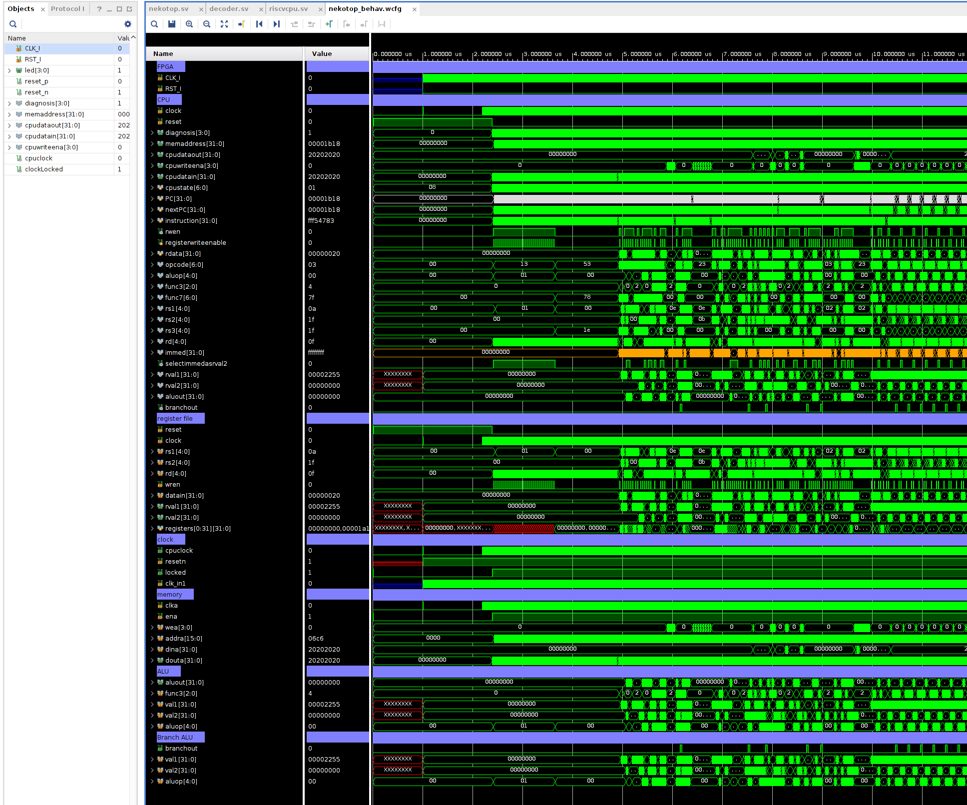
At this point, if we run a simulation, we’ll see that our CPU is now running like clockwork, minus access to these extra devices:

This concludes part 9. In part 10, we’ll add a UART device so we can interact with our little computer.