RISC-V CPU & CUSTOM GPU ON AN FPGA PART 15 – ADDING DDR3 SUPPORT, AND COLOR PALETTE SUPPORT ON THE GPU
BEFORE WE BEGIN
In this part we’ll start talking about DDR3, color palette addition to our GPU.
But before we go further, and since the files are getting too large to post here, we need to grab them from a git repository. Please head over to https://github.com/ecilasun/nekoichiarticle and use the following command to pull the files for all parts of the series:
git clone https://github.com/ecilasun/nekoichiarticle.gitafter creating and changing to a folder of your preference with sufficient free disk space, since this is where we’ll be working on all parts of the series from now on.
Arty A7 and DDR3
So far, we have ignored a very valuable resource that has been sitting idle on our Arty A7 board, the DDR3 chip.
On this specific model (A7-100) the DDR3 chip is a 2Mbit part, which is 256Mbytes of memory for us to use as we please, mainly for storing and executing large programs from, and for keeping around larger chunks of data.
However, the circuitry that the DDR3 MIG7 IP that will generated is not going to be small, and probably be in the order of 4 to 5 thousand LUTs and a whole lot more FFs. However at the end of the day, we’ll be gaining a lot of storage space, so I guess that’s a good compromise.
Another issue that will come up is that the DDR3 interface generates its own clocks and reset lines and assumes the rest of the circuitry will use these. Of course, this is absurd and we don’t really want to step even one Mhz from our CPU speed (100Mhz), therefore we’ll look at some means to achieve this.
And lastly, we’ll need to add some means to stall our CPU until the reads/writes are complete to the DDR3 chip so that we don’t get back corrupt data or accidentally poke the write address while writes are in flight.
Let’s begin!
The Memory Interface Generator
For Arty A7-100T, the FPGA part is xc7a100t-* and apparently does not contain a built-in DDR3 controller. Not to worry though, Vivado 2020.2.2 comes with a suitable DDR3 controller which will work for our purposes.
The project files for part15 already have a memory controller set up, but I think it’s useful to go over it once here to show the key points.
To add a memory controller to our project, we first need to go to the IP Catalog, and select/double click the Memory Interface Generator (MIG 7 Series) entry.
Once the wizard starts up, make sure it shows the FPGA part correctly (xc7a100t as mentioned above) and hit next.

For the next part, pick Create Design and do not check AXI4 interface, since we have our own device router mechanism. Number of controllers should stay at 1 since we need only one.

In the next part, we don’t need to pick a migration part since we are staying on one board.

We pick DDR3 SDRAM and continue forward.

Now this part is not hundred percent clear from the information provided by Digilent on their manual. The Clock Period setting should be set to 3000ps for a 333.33Mhz clock rate which is as advertised. However the Memory Part needs to be set to MT41K127M16XX-15E, which is a 2Mbit part and is compatible with the part advertised on Digilent’s web page (which claims a MT41K128M16JT-125 part)
Make sure the Memory Voltage is set to 1.35V, Data Width is at 16, and leave Number of Bank Machines as is (4 is default in my case)
We need Data Mask to be enabled since we want to be able to do partial writes to memory (such as when writing a byte)
Lastly, the most important one: make sure to set Ordering to Normal or otherwise you’ll be getting a lot of out-of-order operations which will pull the carpet under your feet.

This next page seems to have a bug and keeps forgetting the Input Clock Period setting. Make sure to set it to 6000ps (for a 166.66667Mhz clock), and please make sure to re-set it to 6000ps every time you open the wizard because it will revert back to 3000ps for some reason. Read burst type doesn’t really matter since we’re not doing burst reads, but for now let’s keep it set to Sequential. The Output Driver Impedance Control and RTT both need to be set to RZQ/6 for this part, and Controller Chip Select Pin has to be Enabled.
For convenience, Pick the Bank/Row/Column option for Address Mapping and continue.

For NekoIchi, we’ll be feeding MMCM-generated clocks to the MIG, and not use a device pin. Therefore, we need to select No Buffer for both the System Clock and the Reference Clock.
Reset polarity needs to be LOW for our design, Debug Signals need to be kept off and Internal Vref has to be enabled.
Also unless you want to wire temperature control yourself, make sure to set XADC Instantiation to Enabled. This will ensure that there’s an internal temperature/clock control unit generated so that we don’t get drifts and signal issues with increasing die temperature (and yes it will heat up quite a bit, up to 59 degrees Celcius in my test cases with a heatsink attached, so please make sure to keep some small heat sinks nearby for later installation onto the DDR3 chip)

Next page is simple, just make sure it shows 50 Ohms for the termination impedance, and continute

For the next section, we’ll pick Fixed Pin Out

This will bring us to the Pin Select screen. Easiest way is to go to Digilent’s depot and pull this file from their git page, or grab it from this project link
Once you have the file, click Read XDC/UCF, select it from where you downloaded it, and the window will be populated with device pins matching the signal names in the file.

As you may notice, Next is now grayed out. To be able to continue, we need to hit Validate, which should display the following dialog if everything went well. If not, please cancel the wizard, make a new one and make sure you follow each step and match everything to the screenshots exactly. If all went well, close the dialog using OK, and hit Next (which is now highlighted) to continue.

There’s nothing much to change on the following screen. Leave everything as No Connect and hit Next. This is because we’ll tile internal device wires instead of external pins to these signals.

Rest of the screens are informative and/or show license terms that you need to Accept, so follow those through and finish the wizard. On the last screen, keep the option to generate an Out Of Context IP and we should be ready to use our brand new (and very resource intensive) memory controller.
Wiring the controller
The core of the wiring is quite simple really, the signals named ddr3_* go out to the actual chip, and the signals named app_* tie to our memory interface from the CPU side. The sys_clk_i is tied to a 166.66667 Mhz MMCM clock, and clk_ref_i is tied to another 200Mhz MMCM clock generated using the fpga input clock. Most tutorials claim that 100Mhz signals work and the internal logic etc will handle it, but that is not the case for the setup we’ve done above, as not using the correct clock speeds will directly fail our implementation step and won’t work.
The final wiring looks as below. This memory is marked SLOW below, since it’s actually much slower in response than the internal block RAM.
There are two signals of interest here which require a bit of explaining: ui_clk and ui_clk_sync_rst. Most explanations around these signals give the wrong impression that the rest of the design needs to use these as their clock and reset signals, which is not the case.
What needs to happen with these signals, though, is that a state machine using ui_clk/ui_clk_sync_rst need to drive the interface from our CPU side. But our CPU runs at 100Mhz, and this clock usually ends up being something odd at around approximately 81Mhz, which brings us back to the same clock domain crossing issue from older parts in this series.
// System memory - SLOW section
DDR3MIG SlowRAM (
   .ddr3_addr   (ddr3_addr),
   .ddr3_ba     (ddr3_ba),
   .ddr3_cas_n  (ddr3_cas_n),
   .ddr3_ck_n   (ddr3_ck_n),
   .ddr3_ck_p   (ddr3_ck_p),
   .ddr3_cke    (ddr3_cke),
   .ddr3_ras_n  (ddr3_ras_n),
   .ddr3_reset_n(ddr3_reset_n),
   .ddr3_we_n   (ddr3_we_n),
   .ddr3_dq     (ddr3_dq),
   .ddr3_dqs_n  (ddr3_dqs_n),
   .ddr3_dqs_p  (ddr3_dqs_p),
   .ddr3_cs_n   (ddr3_cs_n),
   .ddr3_dm     (ddr3_dm),
   .ddr3_odt    (ddr3_odt),

   .init_calib_complete (calib_done),
   .device_temp(device_temp),

   // User interface ports
   .app_addr    (app_addr),
   .app_cmd     (app_cmd),
   .app_en      (app_en),
   .app_wdf_data(app_wdf_data),
   .app_wdf_end (app_wdf_wren),
   .app_wdf_wren(app_wdf_wren),
   .app_rd_data (app_rd_data),
   .app_rd_data_end (app_rd_data_end),
   .app_rd_data_valid (app_rd_data_valid),
   .app_rdy     (app_rdy),
   .app_wdf_rdy (app_wdf_rdy),
   .app_sr_req  (app_sr_req),
   .app_ref_req (app_ref_req),
   .app_zq_req  (app_zq_req),
   .app_sr_active(app_sr_active),
   .app_ref_ack (app_ref_ack),
   .app_zq_ack  (app_zq_ack),
   .ui_clk      (ui_clk),
   .ui_clk_sync_rst (ui_clk_sync_rst),
   .app_wdf_mask(app_wdf_mask),
   // Clock and Reset input ports
   .sys_clk_i (sys_clk_i),
   .clk_ref_i (clk_ref_i),
   .sys_rst (resetn)
  );
The above interface’s output clock, ui_clk, drives a small always block in our design, which talks to two domain crossing FIFOs. One of them brings commands from cpuclock domain to the FIFO and are read at the ui_clk speed, and the other one tells us the last read value, written from ui_clk and read from cpuclock domain. This way, we can stay away from using these reset and clock signals which would limit us to slower clocks and the clock path would end up being way too long and eventually not be able to attain timing. We can now happily use our 100Mhz clock for the CPU, and have some small amount of WNS to spare.
It is worth noting here that the total compile time for NekoIchi at this point is 1:40 for synthesis and 5:13 minutes for implementation. This is incredibly short compared to some other variations out there, but there’s no guarantee that we’ll be able to keep the WNS and compile times around these figures permanently, going forward, unless we change our design..

Crossing the clock domain, both ways, in the snow, up hill, with wolves chasing
The inherent delay of DDR3 is only ever going to get worse now, since we need to cross clock domains, twice. Once is for feeding the state machine from cpuclock to ui_clk, and once more to signal the CPU from ui_clk domain that our read or write has complete so we can stop stalling the bus.
This makes the DDR3 so slow that here’s a figure showing the slowdown in real world terms using the DDR3 write test I’ve built to check speed degradation in this scenario. The test first runs code from internal block RAM, and the second time from DDR3 RAM. In both cases, zeros are written to the 256Mbyte DDR3 memory range in a very long loop. Using the built-in wallclock, we can then measure the impact of stalling the CPU for DDR3 reads during code execution while other DDR3 traffic is going on:
# Code in BRAM
Clearing 256Mbytes took 24485 ms (0x000053ED)
Zero-write rate is 12.201257 Mbytes/sec

# Code in DDR3
Clearing 256Mbytes took 272493 ms (0x0004286D)
Zero-write rate is 0.962021 Mbytes/sec
This is a speed decrease of more than 12 times, and is utterly unacceptable, which brings us to the subject of our next article: caching. Luckily, the project files for this part are not yet using the DDR3-first memory layout, so for now we’re save and stay within the 12 Mbytes/sec range.
However, this is still way too slow for DDR3 RAM, since we’re not using the burst modes, and ultimately we should be achieving approximately 180 to 200 Mbytes/sec sustained data rates. We’ll work on this later.
Bus stalls
Majority of the above cost is due to bus stalls during instruction fetch, since we don’t want the FETCH state to move forward with the current instruction before it’s read from DDR3 memory. For cases where the instruction is in BRAM, we don’t get a bus stall signal, therefore execution resumes at expected speed.
If you haven’t done so, please grab the project files here and take a brief look at the DDR3 stall mechanism in the ddr3controller module (at the end of the file):
assign ddr3stall = deviceDDR3 & ((busre&(~ddr3readvalid)) | ((~busre)&(~(mainstate==MAIN_IDLE))));The above wire ties our bus stall state to a few things. First, we need to be accessing the 256Mbyte memory range of DDR3 memory (from 0x00040000 to 0x0FFFFFFFF) which is denoted by the deviceDDR3 bit. After that, we could be either reading or writing. If we were reading, we need to make sure that the read result has fallen through the ddr3read output fifo (valid bit is on when data output is available on the FIFO). For when we’re writing, we need to make sure we made it back to the IDLE state successfully (otherwise, stall).
The stall flag, after being combined with other device’s stall flags, is passed up to the CPU, so it can either stall on FETCH, or on respective parts of the LOAD and STORE states, effectively stopping the CPU until data is available.
This mechanism, even though it looks like it should run at decent speed, is one of the reasons why our DDR3 implementation will run quite slow for a while, since we’ll be stalling for every single instruction fetch. DDR3 interface natively can read 128bit streams, and also work in burst mode to bring lots of data quite fast to the CPU side, and we’ll be exploiting this in the upcoming articles to fill our instruction cache for faster code execution.
Color palette support on our GPU
Now on to a completely different subject. An issue that came up frequently during the development of hardware was the internal color representation versus the output color bit depth.
The DVI interface we utilize for this project uses a 4 bit per component signal, effectively giving us a range of 16x16x16 colors for a total of 4096. However, with the limited bandwitdh internal representation, we were limited to a fixed choice of 8x8x4 colors for a total of 256.
To address this problem, but keep the internal bit count at 8, I chose to go with a color palette approach.
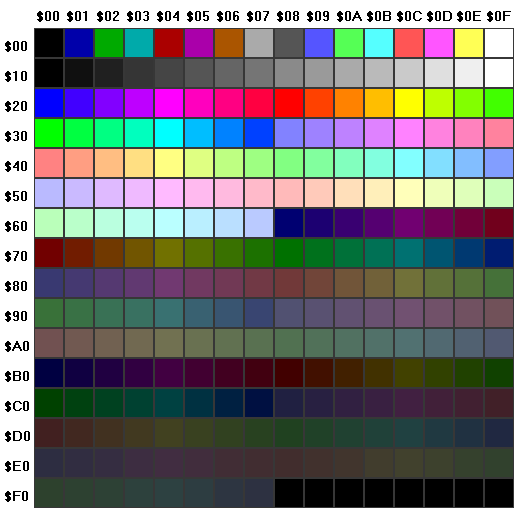
Initially, when NekoIchi boots up, it uses the default VGA color palette as shown here:

Each entry in this table consists of 32 bit values (with top 8 bits to spare) with 8 bit per component representation, which is wider than necessary but this will be good for future support and makes code easier when generating colors.
This palette lives tied to the VideoUnitA/VideoUnitB modules, which now output a color index instead of an RGB triplet. This value is then used to address into the color table, which lets us figure out the RGB color to output to the DVI output hardware.
The great part with this approach is that we can now control the contents of this table to show a subset of 256 colors from our 4096 color palette. The GPU has been augmented with a new instruction to support this, and a C helper function lets us write the color stored in a register over a certain index of the color table:
inline void GPUSetPaletteEntry(const uint8_t rgbRegister, const uint8_t targetPaletteEntry)
{
    // Each color component is 8 bits (8:8:8) giving a 24 bit color value
    // There are 256 slots for color palette entries
    // Color bit order in register should be: ((uint32_t)g << 16) | ((uint32_t)r << 8) | (uint32_t)b) (highest 8 bits are not used at the moment)
    *IO_GPUFIFO = GPUOPCODE(GPUWRITEPALETTE, rgbRegister, 0, targetPaletteEntry);
}
With this approach, and with our additonal DDR3 memory, we can now get fancy images displayed on our screen. Here’s a shot from something we will be looking at running in later articles (please ignore the wrapped around image for now):

Next
We’re at the end of this part. Next time we’ll take a look at ways to optimize DDR3 access by moving instruction fetches out of the way by using an instruction cache.